STM32
Introduction
The timer peripheral is the core part of the SV-PWM driver. It generates the PWM signals that drive the inverter circuit and it also takes care of synchronizing ADC measurements made by the current sampling driver.
The driver is designed to work using one of the advanced control timers,
usually TIM1 and TIM8. They include specific functionalities that are
crucial to have a performant and safe system [STM19].
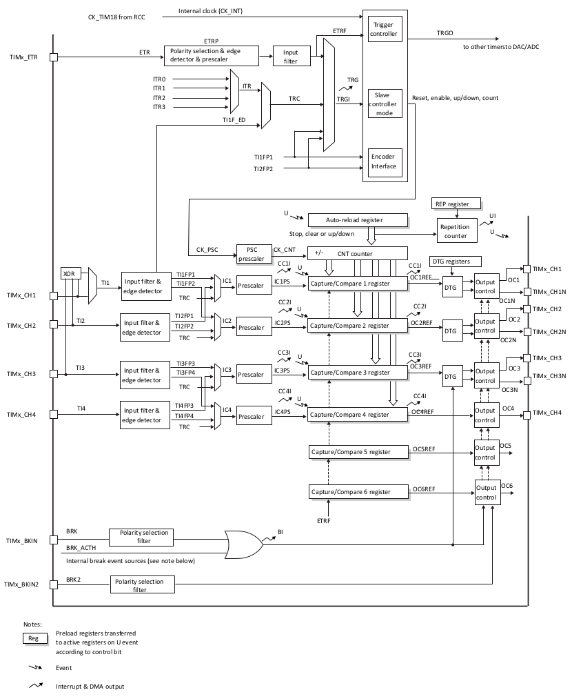
Fig. 17 shows the diagram of an advanced control timer.
PWM generation
The timer peripheral clock, \(\mathrm{f_{TIM}}\), is as fundamental variable
as it controls the timer counting rate. The timer clock is divided by the
prescaler, which is controlled by the PSC register (16-bit). The counting
rate, \(\mathrm{f_{CNT}}\), is defined as:
STM32 timers have multiple PWM modes. The most interesting mode when doing motor control is the center-aligned PWM mode (Fig. 18). In this mode the counting direction (up/down) is automatically alternated by the timer. This mode provides an interesting feature when multiple PWM waveforms are generated such as in a 3-phase inverter. Contrary to edge-aligned modes, in this mode the rising and falling edges of the PWM signals are not synchronized with the counter roll-over. Therefore, switching time varies with the duty cycle value and switching noise is spread. This is a key feature for electric motor drives, since it allows to double the frequency of the current ripple for a given switching frequency. For instance, a 10 kHz PWM will generate inaudible 20 kHz current ripple. This feature also minimizes the switching losses due to the PWM frequency while guaranteeing a silent operation.

Fig. 18 Timing diagram for a timer in center-aligned PWM mode.
Using the above diagram, we can see that the PWM frequency (\(\mathrm{f_{PWM}}\)) is given by:
where ARR is the auto-reload register, a 16-bit value. In order to maximize
PWM resolution PSC should be chosen so that ARR is maximized while
fitting into its 16-bit register.
The PWM duty cycle is controlled via the CCRx registers (x = 1, 2, ...).
CCRx value is compared against CNT so that the PWM signal is active when
CNT < CCRx. In case CCRx is set to zero, the PWM signal is always kept
inactive.
There is an important feature that has to be enabled for CCRx registers:
pre-load. When pre-load is enabled, the register value is only updated when the
timer update event occurs. This is particular useful for real-time control, as
the new register values are applied synchronously. However in center aligned
mode, we have two update events: overflow (at the end of up cycle) and underflow
(at the end of down cycle). Update event happening on overflow should be avoided
since it is the time when current sampling is likely going to occur, and so the
regulation loop. Repetition counter feature comes to the rescue to solve this
problem. In center-aligned mode, odd values of the repetition counter generate
the update event either on overfow or underflow depending on when the repetition
counter register RCR was written and the counter launched. If RCR was
written before starting the counter, the update event will occur on underflow
and on overflow if RCR was written after starting the counter.
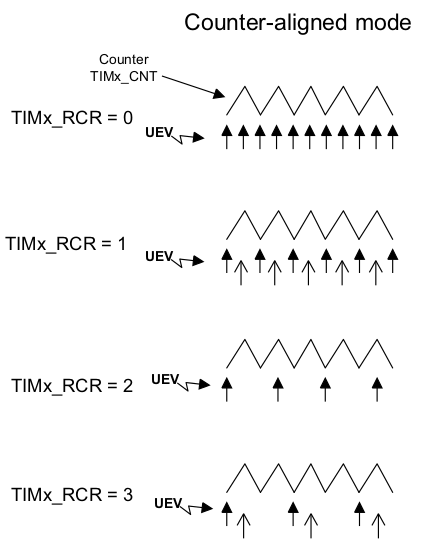
Fig. 19 Example of repetition counter update event generation [STM20].
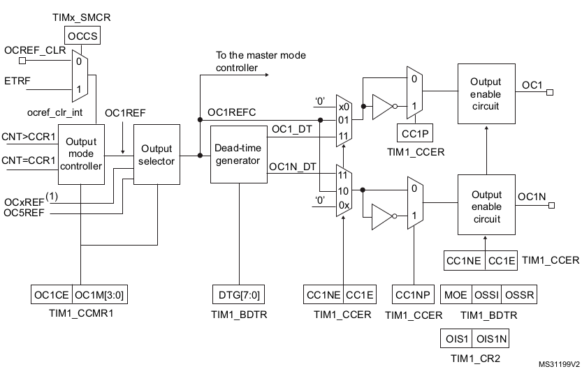
Up to now all the details on the signal generation have been given. The only
missing part is now how to expose these signals to the outside via the OCx
pins. This is controlled by the output stage of the capture/compare channel as
seen on Fig. 20. In general it is necessary to control both
high and low sides of each inverter leg. For this purpose complementary outputs
can be enabled (OCxN). As described in the following section, it is also
possible to insert dead-time when using complementary outputs. Some integrated
drivers do not require complementary signals since they internally take care of
their generation including dead-time insertion.
ADC synchronization
As detailed in the Current sampling page, it is crucial to synchronize the
current measurements with the PWM generation. For this purpose, the driver uses
its fourth channel compare unit (OC4) to trigger the ADC. The value of the
CCR4 register controlling the signal duty cycle is updated every time phase
voltages are set so that currents are always sampled at an optimal point. The
OC4 output is connected to the TRGO output signal. The ADC device
managed by the current sampling driver is responsible to connect to this signal
as a trigger source.
Break function
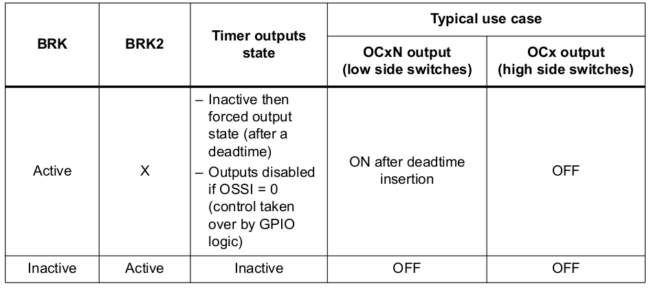
The break function is used to protect the power stage driven by the PWM signals. There are two break inputs which are usually connected to fault signals generated by the power stage circuit (e.g. over-current). When any of the input is activated a hardware protection mechanism is triggered so that the PWM outputs are disabled, leaving them in a pre-programmed state. The break circuitry works asynchronously, that is, it does not depend on any system clock. This feature makes sure that the circuitry does not suffer from any clock propagation delay or system clock failures.
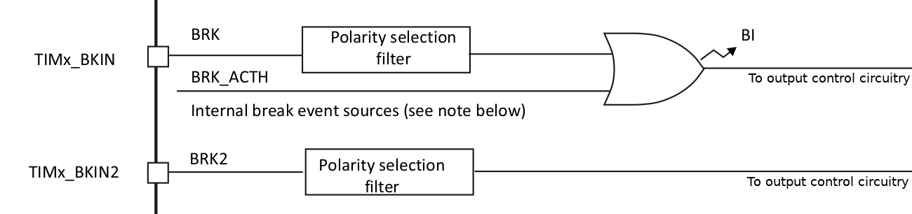
As shown in Fig. 21 BRK is the result of either an
external event (BKIN) or an internal event (BRK_ACTH) such as a clock
failure event (refer to [STM20] for more details). The first channel,
BRK, has priority over BRK2. BRK can also be configured to either
disable (inactive) or force PWM outputs to a predefined safe state. Furthermore,
a dead-time can be programmed to avoid potential shoot-through when activating
the break functionality. This provides a dual-level protection scheme, where for
instance a low priority protection with all switches off can be overridden by a
higher priority protection with low-side switches active. Let’s consider for
instance that the fault occurs when the high-side PWM is ON, while the safe
state is programmed to have high-side switched OFF and low-side switched ON. At
the time the fault occurs the system will first disable the high-side PWM, and
insert a dead time before switching ON the low side.